Difference between revisions of "RoboCup: Control Board 2011"
| Line 21: | Line 21: | ||
== Motor Operations == | == Motor Operations == | ||
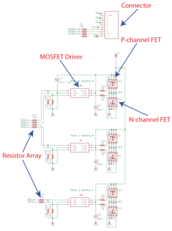
| − | [[File:RC EE three phase bridge 2011 c.png|left|thumb|250px| | + | [[File:RC EE three phase bridge 2011 c.png|left|thumb|250px|'''Figure 1.''' Schematic of a single three-phase bridge.]] |
| − | + | A three-phase bridge ([[:File:RC EE three phase bridge 2011 c.png|figure 1]]) is the name of the circuit that is used to control each motor. | |
=== MOSFET Operation === | === MOSFET Operation === | ||
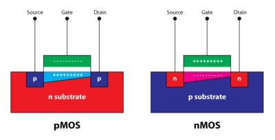
| − | [[File:RC EE Mosfet Diagram.png|right|thumb|400px|MOSFET | + | [[File:RC EE Mosfet Diagram.png|right|thumb|400px|'''Figure 2.''' MOSFET conduction diagram.]] |
| − | A MOSFET or Metal-Oxide-Semiconductor Field-Effect Transistor, is basically a switch. There are 3 terminals: source, drain, and gate. If you apply a voltage at the gate, this will allow a flow of charges from the source to the drain. These devices use metal oxides and the charges flow due to the effect of an electric field between the source and drain. Hence why they are called MOSFET. | + | A MOSFET or Metal-Oxide-Semiconductor Field-Effect Transistor, is basically a switch. There are 3 terminals: source, drain, and gate, and [[:File:RC EE Mosfet Diagram.png|figure 2]] outlines the physical layout of their relations. If you apply a voltage at the gate, this will allow a flow of charges from the source to the drain. These devices use metal oxides and the charges flow due to the effect of an electric field between the source and drain. Hence why they are called MOSFET. |
| − | There are 2 types of MOSFETs, nMOSFET - where the majority of charge carriers are electrons - and pMOSFET - where the majority of charge carriers are holes. The gate-source voltage must be high (positive) to turn on a nMOS and low (negative) to turn on a pMOS. This voltage is refereed to as the threshold voltage and is defined | + | There are 2 types of MOSFETs, nMOSFET - where the majority of charge carriers are electrons - and pMOSFET - where the majority of charge carriers are holes. The gate-source voltage must be high (positive) to turn on a nMOS and low (negative) to turn on a pMOS. This voltage is refereed to as the threshold voltage and is defined in table 1 below. The pMOS is better at pulling the output high while nMOS is better at pulling the output low; Therefore, both MOSFETs are used in the motor driver circuit - they complement one another. |
{| class="wikitable" | {| class="wikitable" | ||
| − | |+ Conduction Requirements | + | |+ <span style="font-variant:small-caps">'''Table 1'''<br />Conduction Requirements</span> |
! nMOS | ! nMOS | ||
! pMOS | ! pMOS | ||
| Line 41: | Line 41: | ||
| <math>V_{G} - V_{S} {\color{red} > } V_{T}</math> || <math>V_{G} - V_{S} {\color{red} < } V_{T}</math> | | <math>V_{G} - V_{S} {\color{red} > } V_{T}</math> || <math>V_{G} - V_{S} {\color{red} < } V_{T}</math> | ||
|} | |} | ||
| − | |||
| − | |||
| − | |||
| − | |||
| Line 51: | Line 47: | ||
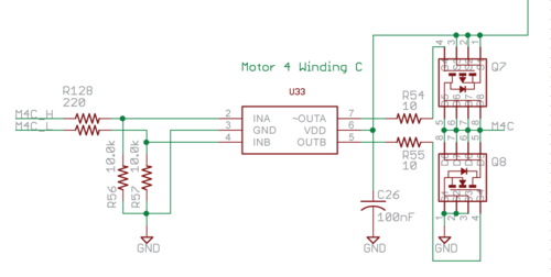
| − | ''OUTA'' is the inverting output and ''OUTB'' is non-inverting output (from the MOSFET Driver). ''Q7'' is the pMOS and ''Q8'' is the nMOS. The source of the pMOS is connected to ''VDD'' (+12V) and the drain is connected to one of the motor coils. In the nMOS, the source is connected to the motor coil while the drain is connected to ''GND''. | + | From [[:File:RC_EE_Motor_Winding.png|figure 3]], ''OUTA'' is the inverting output and ''OUTB'' is non-inverting output (from the MOSFET Driver). ''Q7'' is the pMOS and ''Q8'' is the nMOS. The source of the pMOS is connected to ''VDD'' (+12V) and the drain is connected to one of the motor coils. In the nMOS, the source is connected to the motor coil while the drain is connected to ''GND''. |
| − | [[File:RC EE Motor Winding.png|thumb|500px|Single | + | [[File:RC EE Motor Winding.png|thumb|500px|'''Figure 3.''' Single motor winding for BLDC motors.]] |
| Line 63: | Line 59: | ||
=== Other Websites/Resources === | === Other Websites/Resources === | ||
| − | * Youtube video explaining the operations of brushless DC motors (BLDC) - [http://www.youtube.com/watch?v=ZAY5JInyHXY | + | * Youtube video explaining the operations of brushless DC motors (BLDC) - [http://www.youtube.com/watch?v=ZAY5JInyHXY|youtube.com] |
| − | * PDF about more BLDC motors - [http://electrathonoftampabay.org/www/Documents/Motors/Brushless%20DC%20%28BLDC%29%20Motor%20Fundamentals.pdf | + | * PDF about more BLDC motors - [http://electrathonoftampabay.org/www/Documents/Motors/Brushless%20DC%20%28BLDC%29%20Motor%20Fundamentals.pdf|electrathonoftampabay.org] |
| Line 73: | Line 69: | ||
This is the main stage where the input, ''VDD'', from the battery is converted to the different DC voltage levels required by the various components on the board. To protect the components on the board, 2 things are done: | This is the main stage where the input, ''VDD'', from the battery is converted to the different DC voltage levels required by the various components on the board. To protect the components on the board, 2 things are done: | ||
| − | # The | + | # The kicker's power supply is separated from the rest of the control board. |
# A fuse is used for the kicker power supply and the power supply for the rest of the board. | # A fuse is used for the kicker power supply and the power supply for the rest of the board. | ||
The big, red 10A fuse is for the kicker power supply and goes to the kicker board and the motor driver circuit. As a safety measure, a separate fuse is used on the kicker board as soon as the power supply comes in from the control board. | The big, red 10A fuse is for the kicker power supply and goes to the kicker board and the motor driver circuit. As a safety measure, a separate fuse is used on the kicker board as soon as the power supply comes in from the control board. | ||
| Line 80: | Line 76: | ||
=== LM2734 === | === LM2734 === | ||
| − | LM2734 is a voltage converter that can convert a maximum of 24VDC to different output voltages depending upon how the other pins are connected to the each other and the value of connected passive components. The circuit used to convert VDD to 5V is based on a similar circuit provided in the datasheet. | + | The LM2734 is a voltage converter that can convert a maximum of 24VDC to different output voltages depending upon how the other pins are connected to the each other and the value of connected passive components. The circuit used to convert ''VDD'' to 5V is based on a similar circuit provided in the datasheet. |
The output voltage depends on the biasing values of the resistors R83 and R84 at the feedback (FB) pin. From the reference diagram, the way to calculate output voltage is given by, | The output voltage depends on the biasing values of the resistors R83 and R84 at the feedback (FB) pin. From the reference diagram, the way to calculate output voltage is given by, | ||
Usually, R2 is fixed as 10k?. We need VO to be 5V. Vref is set internally in the IC as 0.8V, so R1 is calculated to be 52.5k?. This is what has been used in the control board circuit. | Usually, R2 is fixed as 10k?. We need VO to be 5V. Vref is set internally in the IC as 0.8V, so R1 is calculated to be 52.5k?. This is what has been used in the control board circuit. | ||
=== MCP1824T === | === MCP1824T === | ||
| − | + | denotes | |
=== Debugging === | === Debugging === | ||
; LM2734 | ; LM2734 | ||
| − | + | : The voltage at the output should be approximately 5V. | |
| − | + | : The voltage at the FB pin should be approximately 4.2V. | |
| − | + | : The input voltage should not exceed 24VDC. | |
; MCP1824T | ; MCP1824T | ||
| − | The input and output voltages should be at a constant value as specified by the schematic. If there is at least a 0.5VDC difference, then it could cause many electrical faults. | + | : The input and output voltages should be at a constant value as specified by the schematic. If there is at least a 0.5VDC difference, then it could cause many electrical faults. |
== Images of Control Board == | == Images of Control Board == | ||
Revision as of 22:34, 2 March 2014
| Timeline | |
|---|---|
| Year | 2013-2014 |
| Versions | |
| Control Board | 2011c |
| Kicker Board | |
| Main Components | |
| MCU | AT91SAM7S256 |
| FPGA | XC3S100E-TQ144 |
| IMU | IMU-3000 |
| Motors | 30W |
| Battery | - |
Contents
Overview
This page contains reference information for the 2011c control boards.
Quick Links
Motor Operations
A three-phase bridge (figure 1) is the name of the circuit that is used to control each motor. The control signals for the motors come from the FPGA (XC3S100E). The robot uses 4 30W three phase brushless motors to maneuver itself on the field. A 5th motor is also used for the dribbler. In order to operate each motor with the needed precision, a brushless motor driving circuit is used for every motor. The motors also contain hall- Each phase of a brushless motor is controlled using 2 transistors. For this application, a MOSFET type transistor is used. Although MOSFET is the appropriate technical name, it is often shortened by simply saying FET. A p-channel MOSFET (IRF9310TRPBF) is used to connect to +12V and a n-
MOSFET Operation
A MOSFET or Metal-Oxide-Semiconductor Field-Effect Transistor, is basically a switch. There are 3 terminals: source, drain, and gate, and figure 2 outlines the physical layout of their relations. If you apply a voltage at the gate, this will allow a flow of charges from the source to the drain. These devices use metal oxides and the charges flow due to the effect of an electric field between the source and drain. Hence why they are called MOSFET. There are 2 types of MOSFETs, nMOSFET - where the majority of charge carriers are electrons - and pMOSFET - where the majority of charge carriers are holes. The gate-source voltage must be high (positive) to turn on a nMOS and low (negative) to turn on a pMOS. This voltage is refereed to as the threshold voltage and is defined in table 1 below. The pMOS is better at pulling the output high while nMOS is better at pulling the output low; Therefore, both MOSFETs are used in the motor driver circuit - they complement one another.
| nMOS | pMOS |
|---|---|
Single Motor Winding Circuit Explanation
From figure 3, OUTA is the inverting output and OUTB is non-inverting output (from the MOSFET Driver). Q7 is the pMOS and Q8 is the nMOS. The source of the pMOS is connected to VDD (+12V) and the drain is connected to one of the motor coils. In the nMOS, the source is connected to the motor coil while the drain is connected to GND.
-down resistors that ensure INA and INB maintain a proper value if there is no signal from the FPGA. R54 and R55 provide signal stability for the base of each FET (the voltage could oscillate back and forth without them). C26 is used to filter out unwanted high frequencies from VDD.
Debugging
If a fuse is blown, then a likely cause is that one of the FETs experienced a high back flow of current and broke. Ideally you should test for faulty FETs with the FET tester. If you are stranded on a deserted island without the FET tester, you can still determine if a FET is faulty or not. The steps for checking both nFETs and pFETs using a digital multimeter are outlined on the testing a MOSFET page. It is recommended to change the entire three-phase bridge (3 pFETs, 3 nFETs and 3 MOSFET drivers) if any 1 part is damaged.
Other Websites/Resources
- Youtube video explaining the operations of brushless DC motors (BLDC) - [1]
- PDF about more BLDC motors - [2]
Radio Operations
Information will be updated later
Power Operations
This is the main stage where the input, VDD, from the battery is converted to the different DC voltage levels required by the various components on the board. To protect the components on the board, 2 things are done:
- The kicker's power supply is separated from the rest of the control board.
- A fuse is used for the kicker power supply and the power supply for the rest of the board.
The big, red 10A fuse is for the kicker power supply and goes to the kicker board and the motor driver circuit. As a safety measure, a separate fuse is used on the kicker board as soon as the power supply comes in from the control board.
Voltage Monitor for kicker
The voltage monitor is a circuit used to measure the voltage at the output of the transformers, since they are in the range of 150V and is a cause of concern for safety if it is exceeded. The main component of the voltage monitor is the analog-to-digital converter, ADC081C027. The type of architecture used in the ADC is an 8-bit Successive Approximation Register (SAR). In successive approximation, the ADC internally has a DAC, a comparator and 8-
LM2734
The LM2734 is a voltage converter that can convert a maximum of 24VDC to different output voltages depending upon how the other pins are connected to the each other and the value of connected passive components. The circuit used to convert VDD to 5V is based on a similar circuit provided in the datasheet. The output voltage depends on the biasing values of the resistors R83 and R84 at the feedback (FB) pin. From the reference diagram, the way to calculate output voltage is given by, R1=(Vo/Vref- Usually, R2 is fixed as 10k?. We need VO to be 5V. Vref is set internally in the IC as 0.8V, so R1 is calculated to be 52.5k?. This is what has been used in the control board circuit.
MCP1824T
The circuit with these ICs are pretty straight forward. They accept a maximum input of 6V and then give a fixed output voltage. The name of the IC denotes the value of the output voltage. For example, in MCP1824ST---1202E/OT gives a 1.2VDC output and MCP1824T-2502E/OT gives a 2.5VDC output.
Debugging
- LM2734
- The voltage at the output should be approximately 5V.
- The voltage at the FB pin should be approximately 4.2V.
- The input voltage should not exceed 24VDC.
- MCP1824T
- The input and output voltages should be at a constant value as specified by the schematic. If there is at least a 0.5VDC difference, then it could cause many electrical faults.
Images of Control Board
**Images will be integrated into the page when uploading the files is stable. Until then, there is a PDF download.
Download the images as a PDF file.
- RC EE control board 2011c 001.jpg
placeholder image
- RC EE control board 2011c 002.jpg
placeholder image
- RC EE control board 2011c 003.jpg
placeholder image
- RC - control board 2011c - back - 001.jpg
placeholder image
- RC - control board 2011c - back - 001.jpg
placeholder image
- RC - control board 2011c - back - 001.jpg
placeholder image
- RC - control board 2011c - back - 001.jpg
placeholder image
- RC - control board 2011c - back - 001.jpg
placeholder image
- RC - control board 2011c - back - 001.jpg
placeholder image
- RC - control board 2011c - back - 001.jpg
placeholder image
- RC - control board 2011c - back - 001.jpg
placeholder image
- RC - control board 2011c - back - 001.jpg
placeholder image
Board Overview Videos
| Board Overview | |
| FPGA Explaniations |
Component List
PDF Download
Sortable Table
**Clink any heading to sort the table rows**


